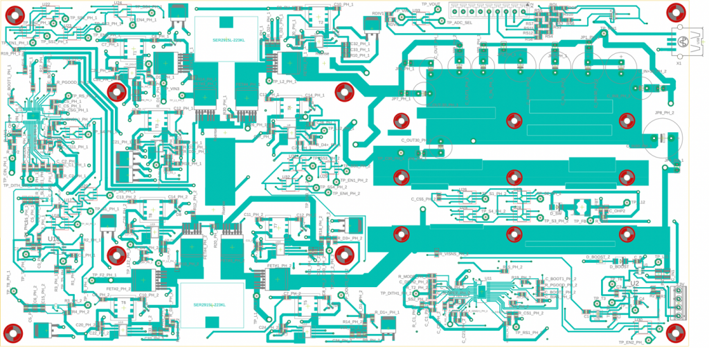
Figure 1: Top layer
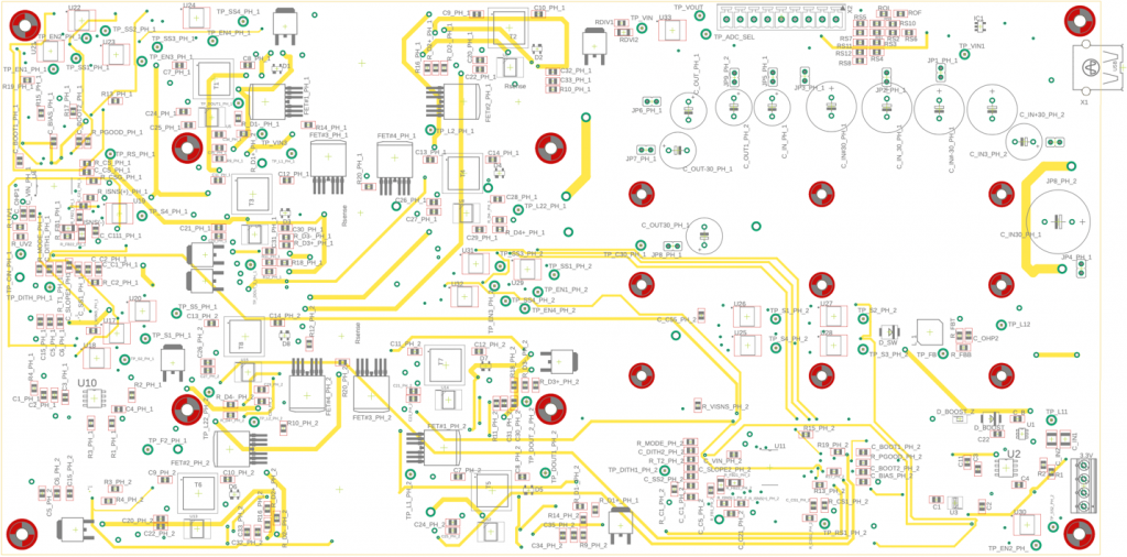
Figure 2: Second layer
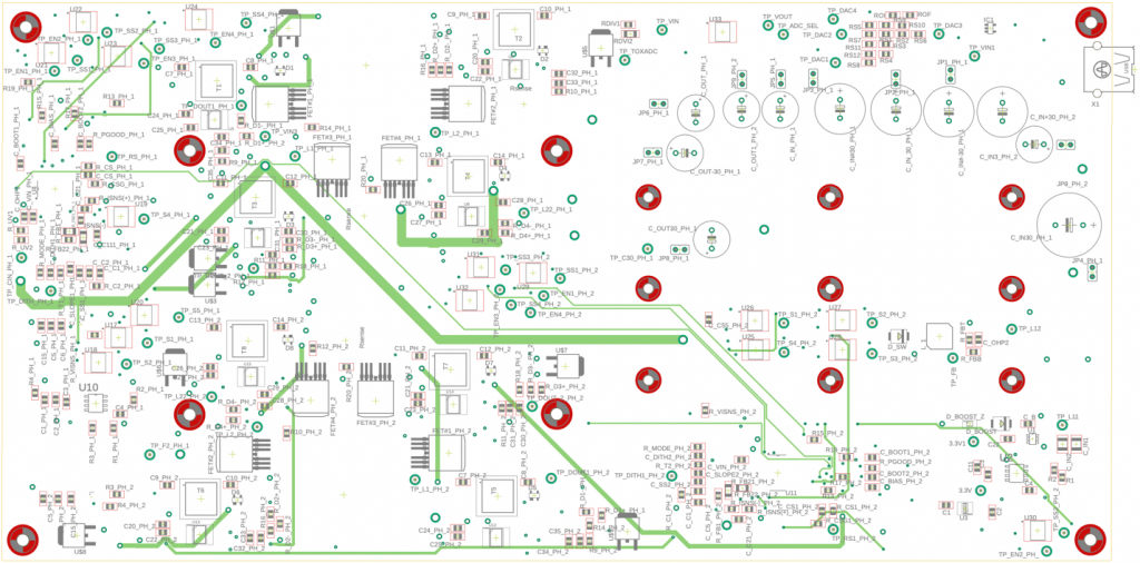
Figure 3: Third layer
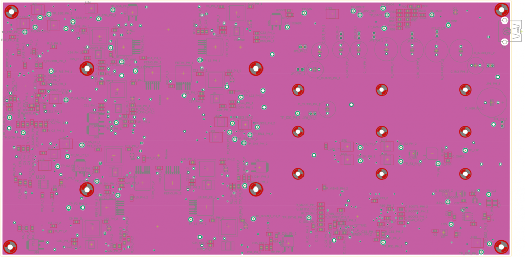
Figure 4: Forth layer (Ground plan)
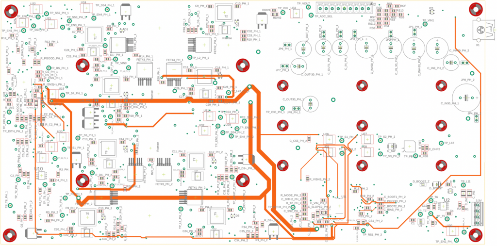
Figure 5: Fifth layer
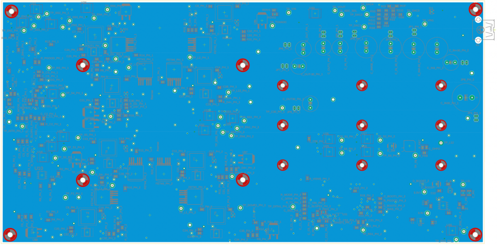
Figure 6: Sixth layer (12V plan/House power)
Figure 1: Top layer
Figure 2: Second layer
Figure 3: Third layer
Figure 4: Forth layer (Ground plan)
Figure 5: Fifth layer
Figure 6: Sixth layer (12V plan/House power)