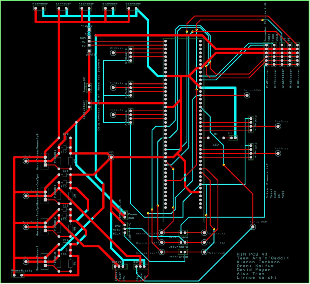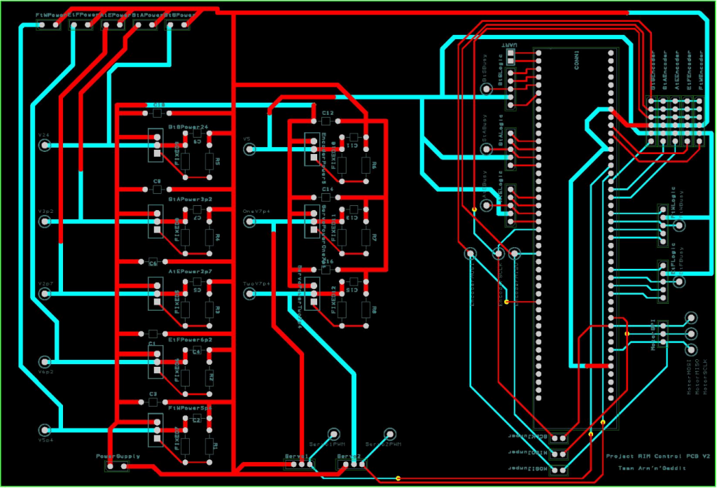
The RIM has run through two PCB (Printed Circuit Board) iterations, each listed below. The current design is using the RIM PCB V2. In order to suit the needs of the arm, each PCB was designed in two parts: Power and Control. These sections were isolated as to reduce the EMI (Electromagnetic Interference) induced by higher wattage traces upon the signal traces in the Control section.
The Power section, found on the left of each PCB, includes voltage regulators, bypass capacitors and terminals for power in/power out.
The Control section, found on the right of each PCB, includes the footprint for the PSoC 6 Protoboard with each pin used for controlling the RIM connected to a breakout footprint.
Both PCB’s feature two layers, as signified by red and blue. The red traces are on the top of the PCB, with the blue on the opposite side. Utilizing these layers allows for a more compact design overall, and typical industrial PCB’s work with 4 to 6 layers to compact their designs further and add greater complexity. The main reasons behind revising V1 and ordering V2 were a set of incorrect footprint sizes, reducing the regulatory circuits from 8 to 4, and adding the capability of powering the PSoC 6 using the board itself instead of the USB connection used for programming the flash memory.